
THE ROADMAP TO A REVOLUTION
Moore’s law has a simple logic to it. The number of transistors in integrated circuits doubles every year.
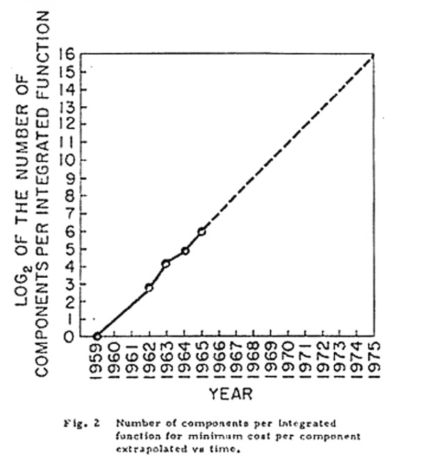
Intel co-founder Gordon Moore made this prediction in 1965. At this time, 50 transistors per chip was the lowest per transistor cost. Moore predicted that, by 1970, an integrated chip would contain 1,000 transistors and that the price per transistor would drop by 90 percent.
This law was a reflection of reality at the time. And it has been a reflection of reality for a long, long time. Indeed, some time ago, the silicon chip industry noticed this trend and started using it as a roadmap for their products. What was a mere observation ended up becoming a target that the entire industry should achieve.
This wasn’t just a goal set by the industry. It became a roadmap for the companies in the semiconductor industry.
The Semiconductor Industry Association, a group that includes Intel, AMD, TSMC, GlobalFoundries, and IBM, started publishing these roadmaps in 1992. In 1998, the group merged with other organizations around the world to produce the International Technology Roadmap for Semiconductors. The most recent roadmap was published in 2013.
For three decades, geometric scaling—shrinking everything on the chip—enabled steady improvements and allowed the industry to be consistent with Moore’s prediction.
Yet Moore’s law wasn’t a rigid rule, Gordon Moore himself had to double the needed time from a year to two years in 1975. In the 2000s, geometric scaling was becoming harder and more difficult to achieve. The industry responded by developing various technical measures such as strained silcons, tri-gate transistors, and new materials to increase capacitance .
But these new techniques seemed to be running into a dead end. To produce the needed chip patterns on the silicon wafers on a smaller scale, light with a 193 nanometer wavelength is used to achieve features at a scale of 14 nanometers. This results in added complexity and costs to production.
The industry is looking at using extreme UV, light with a 13.5nm wavelength, to solve this problem, but its application has run into engineering problems. Even with this technology, further scaling seems to be difficult. At 2 nm, transistors in the chip would be 10 atoms wide and reliable operation seems unlikely. Assuming that this is even solved, power usage and dealing with the heat it releases becomes harder.
All these new techniques took more than a decade to implement and extreme UV has been discussed for far longer. The counterpart to Moore’s law, Rock’s law, states that cost of the fabrication plant for integrated circuits doubles every 4 years.
At this point, should we be surprised that the semiconductor is ready to declare Moore’s law as finished?
Source: Intel
Every improvement in a microprocessor’s performance was expensive for the industry. It meant that they had to develop the technology, techniques, and skills needed to scale the elements of the circuit so that more of them could be jammed on a chip and allow electrons to move between quickly. The boom of Silicon Valley seemed to mitigate this due to the huge quantities sold by the companies. This provided them with enough capital to cover the cost of upgrading to newer technology and still be able to drop the prices for their products.
But as time went on, the chip-making process became more complex with more steps and stages being required. It required that companies be able to synchronize changes to this complex process or else risk stopping progress altogether. This happened to Intel when it planned to switch to 10 nm in processors in 2016 but had to change plans due to problems in their fabrication plans, delaying it to second half of 2017.
An additional problem has that the increase in transistors have not necessarily made it easier to use these chip as the millennium rolled by. Due to heat constraints, only marginal improvements on performance have occurred in the latest chips. While theoretically performance has increased in a processor, software were having difficulties taking advantage of these improvements.
And so it has come to this. The ITRS decided in 2014 that its next roadmap, which will be published next month, would no longer follow Moore’s law and instead take a differing approach.
The industry will move away from focusing on the technology used in the chips and instead focus on a diverse array of sensors and low power processors, a move surely due to the development of smartphones and Internet of Things. The planned chips will go beyond previous chips by including RAM, power regulation, GPS components or gyroscopes, all features widely valued in mobile devices.
It also means that the goal is now much more varied than the previous doubling of transistors set. It means development of new technology needed in production. Materials used are included in this with companies exploring the use of carbon nanotubes and graphenes in microprocessors.
Geometric scaling isn’t necessarily off the books. Instead, the industry is simply holding out for the development of quantum properties, alternative materials and other technologies that could again allow for scaling again.
So for now, Moore’s law is back to a guide. But lest consumers fret, their gadgets and computers will still get more powerful…just not in the same way.
Comments
Post a Comment